


Placement Solutions for Packages Including SiP and Other Module Parts
There is continued demand for the electronic devices we use, such as smartphones and wearable devices, to keep getting smaller while sustaining higher functionality. Also, with the proliferation of the Internet of Things we have reached the point in which communication modules and sensors are now commonplace in our home appliances and cars. This in turn has led to growth in demand for system in package (SiP) and other module parts. A common theme in the production processes for SiP and other module parts is the intertwining of cutting-edge placement technologies such as those for higher density placements, thinner structures, and multilayering.
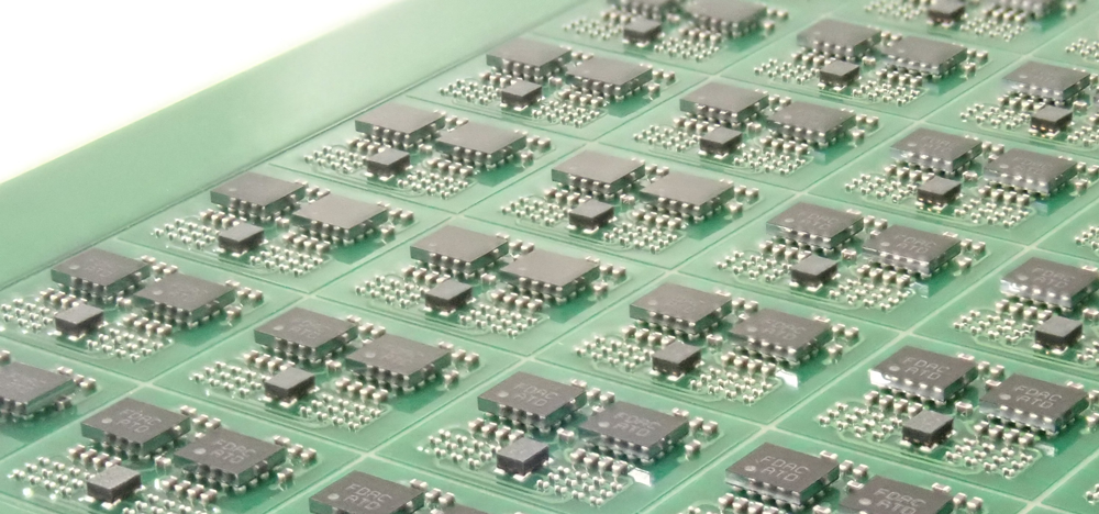
Fuji provides an array of solutions for manufacturing SiP and other module parts. In this article we will be looking at solutions for higher density placements and thinner structures using Fuji functions and units. (Image 1)
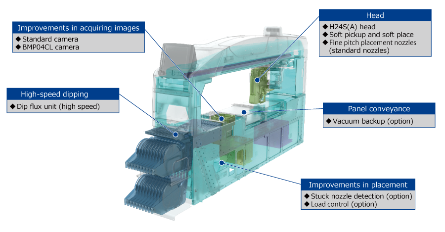
Image 1: Solutions for manufacturing SiP and other module parts
In this section, we will cover issues surrounding placing parts at increasingly higher densities and solutions to these issues.
There is a trend toward having more parts being placed into SiP in order to realize higher functionality for electronic devices. We are seeing examples in which the quantity of parts being placed into RF modules has increased by approximately 20% in two years. Because there are more parts being placed to create each SiP, production takes longer and the quantity of SiP that can be manufactured goes down. This is why there is a demand for higher throughput at the SMT machine to be able to increase the produced quantity.
A high throughput of 42,000 cph (chips per hour) can be achieved using NXT III and an H24S or H24A head with productivity priority mode. It is possible to switch between three different placement modes during placement cycles to match the panel design; productivity priority mode that places importance on productivity, standard mode, and heightened accuracy mode that places greater importance on accuracy.
It is not only passive parts that are increasingly being used for placement in SiP. We are also seeing greater numbers of WLP with small bumps being placed. In a normal process using passive parts, solder paste is printed, parts are placed, and lastly solder is hardened in reflow to establish a firm bond on the panel. However, attempting to print solder for WLP in the same way as solder is printed onto lands for passive parts is difficult because of how small the apertures in the metal mask would have to be for WLP bumps. Increased quantity of parts to be placed Because of this, it is necessary to transfer either solder paste or flux onto the bumps of WLP. The industry is in need of ways to improve the throughput for transfer processes, as well as that for pickup and placement.
Fuji has developed a solution for accelerating the transfer process while using a high-speed rotary head, something that is said to be difficult to do. The maximum throughput that can be achieved for high-speed transfer using H24S or H24A heads is 18,500 cph, which demonstrates a great improvement in productivity. (Image 2)
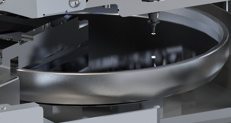
Image 2: High-speed transfer using an H24S or H24A head
As mentioned briefly in the previous section, there are more parts being placed for SiP. However, making the placement area bigger to accommodate this increase in parts will result in the SiP becoming bigger. This in turn means that electronic devices would also have to get bigger. Additionally, there is a push toward smaller populated panels in smartphones to allow for larger batteries. To enable this, there is a trend toward reducing the space between parts for a smaller placement area. To do this, improvements need to be made in placement performance to enable even finer pitch placement.
There are two solutions for fine pitch placements we would like to share.
When placing parts onto panels with fine pitches between parts, there are cases in which the tip of the nozzle may come in contact with an already placed part if the nozzle tip protrudes from the edge of the held part, leading to placement defects. To prevent interference with adjacent parts, it is necessary to ensure that the portion of the nozzle tip that protrudes from the edge of the part is as small as possible. The trend for SiP is often to have part pitches that are 100 μm or less. Sometimes the pitch can be as little as 65 μm. There is an expectation that the space between parts is going to become even narrower. (Image 3)
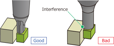
Image 3: Placement next to adjacent part
It is possible to use standard nozzles with fine pitch placement support to keep the portion of the nozzle tip that protrudes from a part edge to a minimum, enabling fine pitch placement. (Image 4)
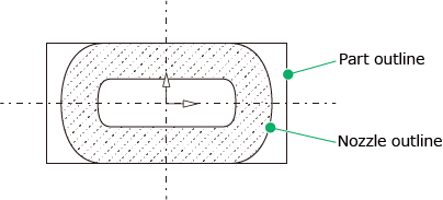
Image 4: Nozzle shape for fine pitch placement
For SiP, filletless soldering is becoming more common for part joints in order to achieve narrower spaces between parts. This is because there is not a mixture of part sizes from small passive parts to large ICs and connectors like what you would see on a motherboard. Also, because the surface onto which parts were placed on an SiP will be enclosed in resin, there are cases in which it is not necessary to ensure strong connection between parts and connection points on the board through soldering. This has led to a trend in which less solder paste is being used. There is less tacking force to hold parts in place on the solder when the amount of solder paste is reduced. So there needs to be a way to have stable part placement under low tacking conditions. (Image 5)
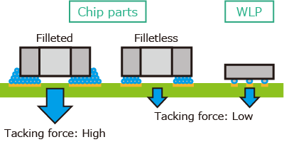
Image 5: Tacking force between part and panel
By using optimum air control with a combination of the NXT III and H24A head during part placement, it is possible to maintain stable placement even under low tacking conditions. It is possible to specify the settings for the timing at which the air is controlled based on each part when using an H24A head. Changing this timing makes it possible to achieve the optimum part placement for the placement conditions. For example, if settings are specified so that the vacuum break is completed at the lower limit before raising the nozzle, it is possible to prevent defects that might occur due to the air released during the vacuum break. (Image 6)
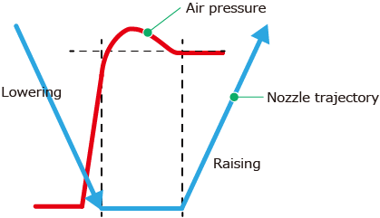
Image 6: Nozzle tip and air pressure
As illustrated in the previous section, the spaces between parts have become narrower to accommodate a smaller placement area, and part sizes have also become smaller for the same reason. The main passive parts placed for SiP used to be 0603 (0201") parts, but more recently they have been replaced with the smaller 0402 (01005") or even smaller 0201 (0.25 x 0.125 mm, 008004") parts. The WLP that are also being placed are seeing a reduction in part size as well. Additionally, in these SiPs, the increased functionality of WLP is resulting in an increase of parts with more pins, as well as parts with smaller bumps. Placement of these very small passive parts and WLP with small bumps requires both high throughput and the capability to place with high accuracy. Some of most important handling capabilities needed for placement of WLP are recognition of very small bumps and the ability to place parts with those small bumps contacting correctly on the panel.
There is a growing trend in bump sizes for the WLP being placed for SiP to be from φ70 to φ100 μm. There are actually a few manufacturers that use WLP that are using bumps even smaller than φ70 μm. A vision processing system with high resolution is required to be able to recognize these small bumps. To be able to place WLP with small bumps, Fuji uses its own servo technology and vision processing algorithm to recognize those very small bumps. This makes it possible to recognize the bumps using a standard camera.
When imaging the bumps on WLP, circuit patterns on the same surface as the bumps may negatively impact the ability to recognize the bumps correctly. BMP04CL cameras have the same functionality as a standard camera, but are able to utilize more sophisticated lighting patterns. By adding colored lights to the lighting, it becomes possible to image and recognize only the bumps. This prevents circuit patterns from being imaged during bump recognition. (Image 7)

Image 7: Effect when changing lighting patterns
After the bumps on a WLP are recognized correctly, the WLP needs to be placed onto a panel. As you can imagine, very small bumps also mean very small lands on the panel. The SMT machine needs to be especially precise to be able to place the part so that the bumps are aligned with the very small lands.
In terms of high accuracy, ±15 μm can be achieved using a combination of NXT III with an H24S or H24A head in heightened accuracy mode, and ±8 μm can be achieved on NXT-H. By optimizing the servo parameters on NXT III, lowering of the throughput can be kept to a minimum. The NXT-H has a high rigidity construction with linear motor movement and high resolution cameras for even higher accuracy.
There is an expectation that SiP will become even thinner in future. This has its own issues that require solutions.
The materials that parts are being made of are changing along with demand for higher functionality. Depending on the material, the impact during placement can cause a great amount of damage to thin parts. It is necessary to reduce the impact load during placement so that parts do not become damaged.
Fuji nozzles have been designed so that the tip of the nozzle is small and lightweight, as well as having moving sections by employing a two-piece configuration, which means that the impact load on parts at the time of placement is reduced. For nozzles used on a high-speed head like H24S or H24A, it is possible to place parts at a low load of 0.5 N without lowering the placement speed. (Image 8)
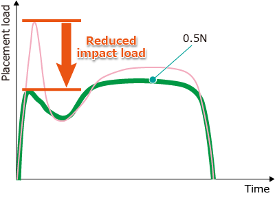
Image 8: Visualization of placement load
Sometimes it is not enough to place parts with a low load onto SiP boards. There is also a requirement to place with an appropriate load for particular parts.
This can be accommodated using a load cell to control the pressure. The placement pressure is controlled by changing the push-in amount. The load is increased by increasing the push-in amount, and the load is reduced by reducing the push-in amount. (Image 9)
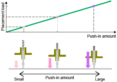
Image 9: Pressure control
While the deflection amount of a spring can be controlled by changing the push-in amount, which in turn allows controlling the placement pressure, because there are variances between the pliability of each spring, those variances can lead to differences in the resulting placement pressure. To ensure the appropriate placement pressure, a load cell is used to measure and compensate for the variances in spring characteristics, improving the accuracy of the placement pressure. (Images 10 and 11)
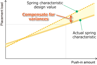
Image 10: Pressure control using a load cell
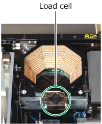
Image 11: Load cell
Periodic maintenance of nozzles maintains nozzle quality. However, if there is a problem during production such as the nozzle becoming stuck, this may lead to parts becoming damaged during placement. This means that there is a demand for being able to check whether nozzles are stuck.
In answer to this, the load cell can be used to detect whether nozzles are stuck, to prevent excess pressure from being applied to parts. (Image 12)
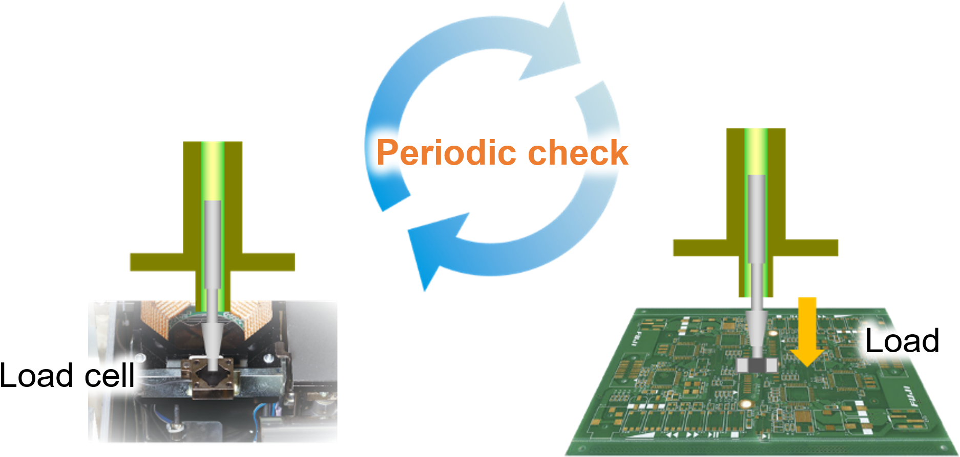
Image 12: Stuck nozzle detection
There is also demand for the ability to lower nozzles at a low speed to keep the impact load when contacting the panel as low as possible, and the ability to raise nozzles at a low speed to prevent parts from remaining on nozzles after placement. Even in these cases, it is still important to keep productivity up as much as possible.
The soft place function makes it possible to use the optimum placement operation for each part. It is possible to individually specify the speed for moving along the Z axis and height at which the speed is changed for either just raising or just lowering operations, or both, when using high speed heads like H24. This makes it possible to apply the required operation just for the parts that require it, keeping the effect on the throughput to a minimum.
As panels become thinner, it is necessary to be able to retain panels while correcting the deflection of the panel and keeping the height of the panel placement surface at a uniform height so that placement quality can be kept stable.
Vacuum backup is effective for retaining thin panels. Vacuum backup uses vacuum pressure to retain thin panels on the upper surface of a vacuum plate to ensure that the part placement surface is at a uniform height. Vacuum backup also helps to reduce the impact of panel warpage and vibrations on the panel from the load to the minimal amount when parts are placed. (Images 13 and 14)
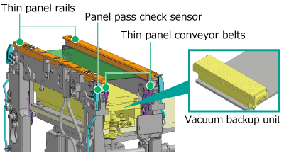
Image 13. Conveyance and clamping of thin panels
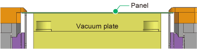
Image 14. Thin panel being held by a vacuum plate
This article has covered many of our solutions for producing SiP and other module parts. In the future, the trends toward increased quantities of placed parts, narrower spaces between adjacent parts, reduced WLP bump size, and thinner parts and panels will continue even further. We are actively working to lead development in these kinds of cutting-edge placement technology for manufacturing SiP and other module parts.